
Semiconductor technology advances high-performance and low-power devices, which is much more critical in applications that include mobile, IoT, and automotive systems. Power efficiency relates directly to battery life, thermal management, and reliability in a system. ASIC designs, on the other hand, are specifically made for tasks, making it either an opportunity or a challenge in terms of low power consumption. The present case study aims to discuss significant methodologies, design techniques, and practical applications in low-power ASIC design.
Introduction
Low power design refers to the strategies and methods employed to minimize dynamic as well as static power consumption in integrated circuits.
As seen from the power equation in Figure 1, low power design minimizes each of its components that in turn lowers the overall power. The equation has both dynamic and static power components:
Dynamic Power is further divided into two:
- Switching Power: Power absorbed while charging and discharging capacitance as the circuit switches between its states.
- Short-Circuit Power: Power supplied for a small period of time when both pull-up and pull-down transistors are simultaneously conducting.
Static Power is mainly leakage current, that flows through the transistors even when there is no switching activity in the circuit.
Static Power depends upon various factors that include:
- Activity
- Frequency
- Transition time
- Capacitive load
- Voltage
- Leakage current
- Peak current
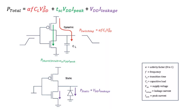
For example, an increase in the voltage will lead to higher power consumption in all components, hence a greater overall power usage. On the other hand, a reduction in the voltage reduces the overall power consumption. Optimal performance and minimal power use are thus achieved by careful trade-offs of these factors using different low power design techniques and methodologies.
Why we need Low Power Design?
Companies are constantly striving to innovate and introduce new features and functionality into portable, handheld, and battery-powered devices. Minimizing power consumption is an important factor for these products as it directly relates to battery life, which is a key differentiator for end users. Long battery life enhances the usability of these devices, while reducing the time it takes to transition from OFF/SLEEP to ON/ACTIVE states ensures a seamless user experience, which is equally important.
For “plug-in” devices, power consumption is still a significant issue since it affects the system’s cost. High power consumption may require extra components, such as heat sinks and advanced cooling systems, and increases electricity costs. For instance, in large-scale server farms using massively parallel systems, the saving in the power consumption of even a single chip translates into a large saving across the entire system. Upgrading such configurations with more advanced, yet power-efficient ICs can greatly reduce both the consumption of power and costs of running operations.
Importance of Low-Power Design
As electronic gadgets have become ubiquitous in today’s circumstances, there is an increasing demand for power-efficient solutions. Battery power is only one aspect of low-power design, it also encompasses reduced heat generation which impacts a device’s reliability and lifetime. For application-specific integrated circuits (ASICs), power efficiency becomes one of the core design constraints to focus on without degrading the performance.
It is a critical consideration of power consumption in ASIC, especially in terms of heat dissipation, performance, and battery life in portable devices. It is categorized into three primary components:
- Dynamic Power
Dynamic power is the largest power consumer in the digital circuit during its operation. It arises from the charging and discharging of load capacitances during the switching action of transistors. The formula for dynamic power can be stated as follows:
Where:
α = switching activity factor
= Load Capacitance
= Supply Voltage
f = Opening frequency
This equation indicates that dynamic power consumption increases with increased switching activity, higher capacitance, a greater supply voltage, and higher frequency. Any of these factors can be decreased to lower the dynamic power consumption.
- Static Power
Static power is known as leakage power. It is the power that is absorbed by the circuit when it is on but not switching. Leakage currents in the transistors cause this loss in power. The two major types of leakage are as follows:
- Sub-threshold Leakage: The current is passing even when a transistor is off.
- Gate Oxide Leakage: Caused by tunneling current through the gate oxide layer.
- Junction Leakage: Caused by reverse-biased p-n junctions of transistors.
With technology scaling down (e.g., smaller transistor areas), leakage power grows because the oxide layers are thinner and components are farther apart.
- Short-Circuit Power
Short-circuit power occurs during the transition period of CMOS gates when both NMOS and PMOS transistors are conducting for a short period. This happens when the input changes, thus creating a direct current path between the power supply and the ground for a short period. The power consumed during this short period is called short-circuit power. It depends on the rise and fall times of the signals, the supply voltage, and the output load.
Click here to learn about “5 Key Factors to Consider When Choosing the Right ASIC Design Technology”.
Key Drivers for Low Power Design:
- Easy Portability of the Device
The current generation of mobile and wearable devices consumes power in efficient ways. Since they are always used on the go, a higher battery life means more usage with less recharging; therefore, low power design is very critical in creating the demand. Users get to reap portability and convenience.
- Sustainability
The reduction in power consumption contributes directly to environmental sustainability. Lower energy usage reduces the carbon footprint of electronic devices, thus reducing strain on natural resources and environmental impact. This corresponds to global efforts in promoting green technology.
- Thermal Management
Reduces the amount of heat generated from electronic components with efficient power consumption. This has not only minimized the thermal loads on devices to enhance their reliability and lifespan but also helped stabilize performance since overheating conditions tend to cause systems to fail or deteriorate to less than an acceptable level.
- Regulatory Compliance
Governments and regulatory bodies around the world impose strict energy efficiency standards. Adopting low-power design ensures compliance with these regulations, which helps manufacturers avoid penalties and maintain market competitiveness while also meeting consumer expectations for energy-efficient products.
Techniques for Low-Power ASIC Design
- Voltage Scaling
Supply voltage can be reduced significantly as it has a quadratic dependence on voltage. This leads to significant dynamic power reduction. Dynamic voltage scaling and multi-voltage domains allow designers to optimize power for different blocks in the ASIC.
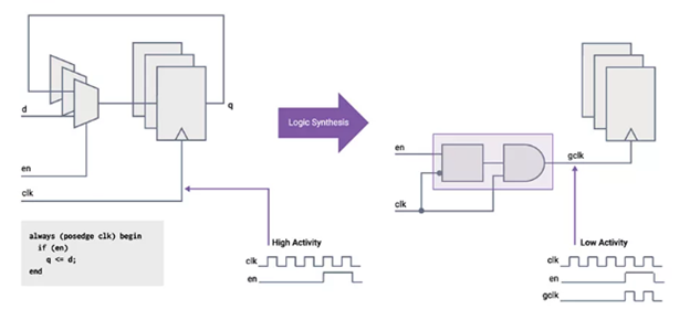
- Clock Gating
This technique of conversion of the enable flip flop during logic synthesis, saves a considerable amount of area for a multiplexer-mux-and can decrease the amount of switching activities overall on a clock network that was shown as figure 2. From the aspect of power minimization, what’s desired from it is reduced capacitive loads-thru lessened area-and activity factors, by reducing the factor that contributes switching power to overall dynamic power. This is a direct and widely applicable approach for optimization of power and area. It depends on how good the synthesis tool is in doing the optimization; fortunately, the technique is mature and well supported in most of the modern design tools and workflows.
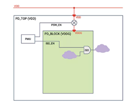
- Power Gating
Power gating is a technique that partitions the functions of an integrated circuit (IC) into power domains, similar to multi-voltage designs. However, in this case, the power supplies for these domains are connected to power switches (see Figure 3). This approach allows power to be completely shut off to a specific block, effectively reducing its voltage to zero. By doing so, power gating eliminates both static and dynamic power consumption for the duration the block remains off.
This technique provides the most significant power savings, making it ideal to shut off as many power domains as possible, as frequently as possible, while still maintaining overall system functionality. To implement power gating, the design must include:
- Power Switches: These physically disconnect the power supply to the designated domain.
- Isolation gates: These ensure the boundary signals are clamped at known values such that the remaining part of the circuit does not display erratic behavior.
- Power Management Unit (PMU): The PMU controls the power switches and isolation enable signals, managing the transition between ON and OFF states.
Sequencing of the PMU signals in the proper manner during power down and power up is essential to make sure that all the signals within the domain are clamped correctly and restored back to normal without errors.
- Multi-Vth Design
Transistors having different threshold voltages or Vth reduces speed and leakage power. High-Vth transistors have less leakage but low performance, while low-Vth transistors are faster but leak power more. The mixed-Vth approach optimizes the power and performance.
- Dynamic Frequency Scaling
Dynamic adjustment of an operating frequency of ASIC with the requirements of the workload. Reduces or consumes power when full performance is unnecessary. Reduces leakage and standby power.
- Activity-Based Optimization
Optimized logic design, signal encoding, and data path management help in reducing dynamic power by minimizing switching activity. Operand isolation and data gating are two effective techniques.
- Low-Power Memory Design
Memory blocks often dominate the ASIC power consumption. Techniques such as memory banking, retention modes, and low-power SRAM design reduce memory-related power.
Challenges in Low-Power ASIC Design
Although low-power ASIC design offers several benefits, it poses some challenges as well:
- PPA Trade-Offs
- Reduction of power often results in degradation of performance and area of the chip. The designer has to strike a balance among these factors so that the project requirement is satisfied.
- Design Complexity
- Power gating and multi-voltage domains add to design and verification complexity.
- Leakage in Advanced Nodes
- At 7nm and 5nm, leakage power becomes a major contributor and demands innovative solutions.
- Verification and Testing:
- Functional correctness and stability across a variety of power modes add to the verification workload.
Future Trends and Innovations
- FinFET and GAA Technologies:
- The advanced transistor architectures, FinFET (Fin Field-Effect Transistor) and Gate-All-Around (GAA), allow for better leakage control and low power consumption in modern ASIC designs.
- AI-Powered Design Optimization:
- Machine learning algorithms are used to optimize power, performance, and area at the design phase.
- 3D ICs and Heterogeneous Integration:
- The stacking of dies vertically and integration of diverse technologies in a single package reduce interconnect power and enhance performance.
- Near-Threshold Computing:
- Operating transistors near their threshold voltage offers tremendous power savings but is challenging in terms of reliability.
Related Insights: Learn how innovations like AI-specific chip architectures accelerate development in Chip Design Innovations for the Age of AI and Machine Learning.
Conclusion
Low-power design in ASIC chips is a must for modern electronic systems, especially in power-sensitive applications. The combination of voltage scaling, clock and power gating, and optimized memory architectures can help designers achieve significant power savings without sacrificing performance. As technology advances, new methodologies and innovations will further push the boundaries of power efficiency, enabling the next generation of energy-efficient devices.
With a rich experience in VLSI, FPGA, and ASIC design, Nanogenius Technologies is helping Indian manufacturers develop and produce top-notch products. Nanogenius enables Indian people to overcome challenges and, in turn, drive innovations to make India a major player in semiconductor technology on the global map.