
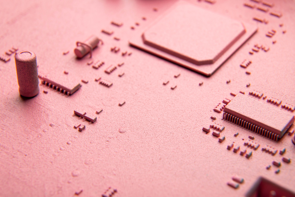
India Archives is becoming more accepted for multilayer PCB design and manufacturing. Multilayer circuit boards promise high-density interconnections, good signal integrity, and performance improvement in areas such as consumer electronics, medical devices, and aerospace. Manufacturing multilayer circuit boards can be challenging. One wrong conclusion by an engineer, and one can expect a lot of delay, cost overruns, and development extensions as well.
If you’re a professional, designer, or amateur who is looking to learn more about PCB circuit design on multilayer boards, you are in the right place! Let us dig into the specifics that need to be taken care of, to come up with a reliable, functional and cost-effective PCB design.
- Understanding the Need for Multi-Layered PCBs
In today’s world, compact and high-performance electronic devices like smartphones, IoT gadgets, and automotive systems demand multi-layered PCBs. Unlike single or double-layer PCBs, multi-layered boards:
- Offer greater routing density.
- Enhance signal integrity with controlled impedance.
- Reduce electromagnetic interference (EMI).
- Improve thermal management.
Modern smartphones with 5G capabilities, for instance, need 8-layer or even 12-layer PCBs to support sophisticated RF circuits, power distribution networks, and high-speed signal transmission. A conventional two-layer PCB would not be sufficient!
Appropriate standards should be taken as acceptable by any manufacturer before putting into production such complex PCBs-a good PCB design house that would optimize the cost and reliability while ensuring that the designs conform to the industry standards such as IPC-2221, IPC-6012, and MIL-PRF-31032. Learn more about PCB design standards here.
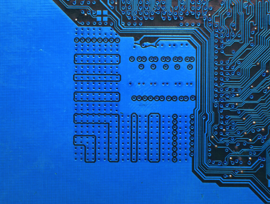
- The Stack-Up
The stack-up defines the number and arrangement of conductive layers and insulating dielectric materials. A well-designed stack-up is essential for:
- Minimizing crosstalk between adjacent traces.
- Maintaining signal integrity in high-speed circuits.
- Enhancing power integrity by reducing voltage fluctuations.
A typical 4-layer PCB stack-up looks like this:
- Top Layer (Signal)
- Inner Layer 1 (Ground Plane)
- Inner Layer 2 (Power Plane)
- Bottom Layer (Signal)
An 8-layer or 10-layer PCB is deployed in high-speed applications like PCIe and DDR4 RAM modules, where stable power delivery and minimum EMI are paramount.
Real-Life Example: Consider an automotive LiDAR sensor PCB. It requires multiple layers for RF signal processing, power planes, and high-speed data transmission. Any miscalculated layer arrangement can lead to malfunctioning sensors, affecting autonomous vehicle performance. Explore how stack-ups impact high-speed PCB design.
- Heat Management
The biggest problem comes when you start stacking up many layers because heat dissipation then becomes a major issue. If not managed properly, excessive heat can lead to:
- Component failures due to overheating.
- Increased electromagnetic interference (EMI).
- Reduced PCB lifespan.
Here’s how to handle thermal management effectively:
- Use thermal vias: They are small copper-plated holes that conduct electrical and heat from hot components to the corresponding external heat sinks.
- Choose metal core PCB (MCPCB): These PCBs use aluminum and copper cores for much better heat dissipation.
- Deploy heat-spreading copper pours: This equally distributes heat across the board.
Read more about thermal management techniques in PCB design.
- Impedance Control and Signal Integrity
When working on high-speed circuits, signal integrity is to be taken into consideration. This obstruction must be provided to the circuit for a working connection; this is done primarily by matching impedances accordingly. Hence, some important points are given below:
- Impedances must be controlled. These will be transmission lines with signals greater than 50 MHz.
- The Trace should be Shorter to avert signal attenuation events and enhance performance.
- Differential pairs are employed in USB, HDMI, and Ethernet circuits, thereby reducing noise.
Real-life example: In high-frequency PCBs for 5G base stations, impedance mismatches can cause losses in the signals, and all these lead to poor network connections. Such PCB design must be simulated by the engineers using PCB design tools such as Altium Designer or Cadence Allegro to ensure controlled routing. Check out how to design PCBs for high-speed signals.
- Design for Manufacturing (DFM)
Despite how advanced your design may be, it must be manufacturable. Designs for Manufacturing (DFM) guarantees that the PCB can be manufactured efficiently and without errors.
Key DFM Guidelines:
- Maintain minimum trace width and spacing based on fabrication capabilities.
- Keep drill hole sizes within the manufacturer’s specifications.
- Minimize vias where possible to reduce complexity.
- Avoid sharp PCB corners, which can lead to stress fractures.
Case Study: A company designing IoT-based wearables initially opted for a 10-layer PCB but later optimized the design for a 6-layer PCB, reducing manufacturing costs by 30% without affecting performance. Explore how DFM saves time and costs in PCB manufacturing.
- Choosing the Right PCB Manufacturer in India
With India emerging as a global hub for electronics manufacturing, choosing the right PCB design and manufacturing company in India can make all the difference.
Look for manufacturers that offer:
- Advanced fabrication techniques (HDI, via-in-pad, blind/buried vias).
- Quick prototyping services for faster development cycles.
- IPC Class 3 Certification for high-reliability PCBs.
- Cost-effective bulk production without quality compromises.
Find the best PCB manufacturing services in India.
- Power Distribution Network (PDN) Design
Well-designed PDNs ensure that all components are fed with stable power devoid of noise, such as peaks and troughs, especially high-speed digital and RF circuits. Poor PDN design can cause:
- Voltage fluctuations lead to unstable circuit performance.
- Power rail noise degrades signal integrity.
- Excess heat affects component longevity.
Best Practices for PDN Design:
- Use solid copper planes for power and ground instead of traces.
- Reduce inductance in power paths by using multiple vias.
- Place decoupling capacitors close to power pins to minimize noise.
- Simulate PDN behavior using tools like Ansys SIwave or Keysight ADS.
Real-Life Example: High-performance FPGA-based boards require multiple power rails. A poorly designed PDN can lead to unstable clock signals, affecting data processing in AI accelerators and autonomous vehicle systems.
Read more on PDN design for high-speed PCBs.
- EMI/EMC Considerations
Investigating the new challenges posed by EMI and EMC has been an issue since the advent of RC circuits. Their impact on the multilayer structure of PCB, especially for IoT aerospace, and automotive applications, has led to qualitative importance.
How to Reduce EMI/EMC Issues?
- Use ground planes to shield signals and reduce loop areas.
- Implement differential pair routing for noise reduction (e.g., USB, HDMI, PCIe).
- Maintain proper PCB trace spacing to avoid crosstalk.
- Use ferrite beads and shielded components in power lines.
Case Study: A medical device manufacturer faced unexpected failures in hospital environments. After analysis, it was found that EMI from nearby machines was interfering with the device. By optimizing grounding and shielding, the design was successfully EMC-compliant.
Explore EMI shielding techniques for PCBs.
- PCB Testing and Validation
Before mass production, rigorous PCB testing is essential. Even a minor design flaw can lead to costly product recalls.
Important PCB Testing Techniques:
- Automated optical inspection, or AOI, finds missing or misaligned parts.
- The flying probe test looks for openings, shorts, and improper connections.
- Boundary Scan Testing: For intricate PCBs with fine-pitch integrated circuits and BGA.
- Thermal testing: Verifies appropriate heat dissipation in practical settings.
For example, the flight control PCB of one drone manufacturer underwent extensive heat and cold testing (-40°C to 85°C) to ensure reliability in various climate conditions.
Read about advanced PCB testing techniques.

- Prototyping and Manufacturing
With this, we move toward prototyping and large-scale production after the printed circuit board design has been finalized and tested.
Steps in PCB Prototyping & Manufacturing:
- Prototype Run: Small batches to validate design performance.
- Design Iteration: Fix issues before large-scale production.
- Mass Production: Choose the right PCB design company for high-volume manufacturing.
For those looking for PCB design and manufacturing in India, ensure that the manufacturer supports:
- HDI PCB fabrication for compact designs.
- Multi-layer PCBs (up to 16+ layers) for high-end applications.
- Quick-turn PCB prototyping to accelerate development cycles.
Find the best PCB prototyping services in India.
- Things to Look for When Selecting a PCB Design Company
A seasoned PCB design firm is essential if you’re working on a high-speed, multi-layer PCB project. What to look for is as follows:
- proficiency with sophisticated routing techniques for multi-layer PCBs.
- EMI/EMC compliance and high-speed signal integrity simulation capabilities.
- complete assistance from design through manufacture and prototyping.
- certifications based on industry standards (IPC, ISO, MIL-SPEC).
Find a trusted PCB design company for your next project.
FAQs
- What advantages does multilayer have over single-layer boards?
The advantages of multilayer boards are higher circuit density, improved signal integrity, enhanced EMI shielding, and improved power distribution capabilities. Most suitable for high-speed electronics, telecommunications, and aerospace applications.
2. How can I reduce expenses while designing a multi-layer PCB?
To optimize costs:
- Minimize layer count by efficient routing and stack-up optimization.
- Choose standard board materials instead of high-end RF laminates unless necessary.
- Work with experienced PCB design companies that offer DFM (Design for Manufacturing) guidelines.
3. What is the typical lead time for manufacturing multi-layered PCBs?
The lead time varies based on complexity and layer count:
- 4-layer PCBs: 5-7 days for prototyping, 2-3 weeks for mass production.
- 8-layer PCBs: 7-10 days for prototyping, 3-4 weeks for mass production.
- 12+ layer PCBs: This can take 4+ weeks due to complex fabrication processes.
Learn how to reduce PCB manufacturing lead times.
Concluding remarks
The knowledge of power distribution, EMI/EMC issues, signal integrity, and manufacturability shall be such as to enable you to design your multi-layered PCBs sensibly. Working hand-in-hand with one of India’s top PCB design and manufacturing companies and adhering to best practices would give you a high degree of confidence in the PCBs dedicatedly developed for novel applications.
For additional information on EMI mitigation, signal integrity analysis, and high-speed PCB design, please check NanoGenius Technologies. Stay updated with the latest developments in this rapidly evolving field!