
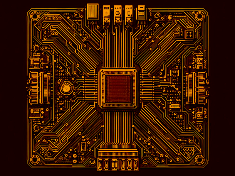
Case Study: ASIC Design Techniques for Multi-Processor System-on-Chip (MPSoC) Development
Today, with the advancement of technology at such a rapid pace, numerous applications need faster and more power-efficient systems. Among them, Multi-Processor System-on-Chip (MPSoC) is one of the principal architectures existing in fields from mobile devices to high-performance computing and automotive systems. The design of an MPSoC is an extremely complex challenge that requires incorporating several processors, memory units, I/O controllers, and custom accelerators on a single chip.
This case study goes deep into the main ASIC design techniques that allow the development of MPSoC, including challenges, methodologies, and real-world applications that expose the effectiveness of the techniques.
Challenges in MPSoC Development
1. Complexity of Integration
MPSoCs contain different components, from general-purpose processors to domain-specific accelerators, and to the shared resources such as memory and interconnects. One of the major challenges is to have efficient communication and synchronization among these components.
2. Power and Thermal Management
As the numbers of processors increase in an integrated circuit, so will their power consumption and heat generation. Managing such parameters is very important to achieve system reliability and efficiency in mobile and embedded systems.
3. Verification and Validation
This adds complexity to MPSoCs, making functional verification challenging. Advanced simulation and emulation techniques are involved in the process of ensuring that all components work together correctly.
4. Scalability and Performance Bottlenecks
Scalable interconnects and memory architectures must be designed to accommodate more and more cores. Data transfer bottlenecks can undermine performance very significantly.
ASIC Design Techniques for MPSoC Development
1. Partitioning and Modular Design
Partitioning of the system into modular blocks is an elementary technique in MPSoC design. Such blocks can denote processing units, memory units, or other custom accelerators.
Advantages:
- The modular structure simplifies design and verification by reducing the system to an easy-to-manage number of components.
- Modular design makes possible the reuse of IP (Intellectual Property) cores from project to project.
ARM’s big LITTLE architecture applies modular design principles to put high-performance and power-efficient cores within one MPSoC.
Click here to know about “5 Key Factors to Consider When Choosing the Right ASIC Design Technology”.
2. Network-on-Chip (NoC) for Interconnect
As the count of cores in MPSoC designs continues to scale, traditional bus-based interconnects face significant challenges. Such simple interconnects are very effective for a small number of cores but tend to become bottlenecks as the numbers of components grow due to scaling issues, bandwidth, and latency requirements.
NoC appears as a high-end interconnect solution to resolve these problems. NoC is an organization of the communication framework of an MPSoC like a computer network within a single chip, which offers scalable and efficient methods for different cores, memory units, and accelerators for smooth communication.
Key Features of NoC
Packet-Switched Communication: NoC uses packet-switched data transfer, similar to data that is routed across the internet. Data is split into smaller packets, then each one routed independently across the network. This means that:
Packet-switched communication provides High Throughput Since several independent packets can be transmitted simultaneously using different routes and allows maximum data transfer rates. Low Latency: Due to no bottlenecks in packet-switched communication, the latency of the bus-based systems is removed.
Parallel Communication: NoC enables simultaneous communication between multiple cores. While on a bus, only one core can send data at a time, on NoC, multiple data streams could pass across the chip in parallel. This is crucial for MPSoCs that will need to have many cores and accelerators work well together.
Real-World Use: Advanced MPSoCs like NVIDIA’s Tegra series employ NoC architectures to manage communication between GPUs, CPUs, and memory.

3. Low-Power Design Techniques
Since these chips are targeted for power-sensitive devices like smartphones, IoT systems, etc., low-power design techniques can become an important aspect of ASIC designs in MPSoCs. The advanced techniques used include reduction of power and performance at the same time.
Dynamic Voltage and Frequency Scaling: It is an adaptation technique which changes the voltage as well as frequency of processor cores according to their workload. In lighter tasks or idle time, voltage and frequency are reduced significantly, cutting power consumption considerably.
Power Gating: Switch off entire unused cores or components so that leakage power is strictly minimized and only active parts consume energy.
Clock Gating: This technique involves disabling the clock signal to inactive components, which avoids dynamic power without an adverse effect on functionality.
For example, Qualcomm Snapdragon MPSoCs use DVFS power gating in combination for the enhancement of energy efficiency as well as extending battery life and make them suitable for portable systems inside the smartphone.
4. Memory Subsystem Optimization
A high-performance design for MPSoC requires an efficient memory subsystem because, almost directly, it reflects on the overall data access speed and system throughput. Several techniques can be used to optimize memory:
Multi-Level Caches: Several levels of cache (L1, L2, and sometimes L3) are used in the MPSoC. Caches help store frequently accessed data closer to the processing cores with reduced latency and minimizes the load on slower main memory, thereby speeding up overall operations.
Scratchpad memory: Dedicated high-speed memory blocks are set aside for specific purposes, improving the access speed for critical data and minimizing reliance upon accessing slow external DRAM that is very power consuming.
Coherency Protocols of Memory: In multi-core systems, MESI (Modified, Exclusive, Shared, Invalid) are memory coherency protocols for supporting simultaneous access to shared memory by multiple cores.
For instance, Apple’s M-series silicon uses a unified memory architecture in which the processors and the GPUs share a pool of common memory. This design improves both performance and energy efficiency by reducing data duplication as well as transfer delays.
5. Hardware Accelerators
Hardware accelerators are integrated into MPSoC processes, specialising workloads including AI inference, video processing and encryption. Such accelerators help offload specific workloads from general-purpose processors in order to improve performance alongside energy efficiency.
Custom Design: These accelerators are designed specifically for special-purpose workloads such as image recognition or cryptographic functions and are therefore optimized for a particular workload to offer some specific performance level that’s beyond what general-purpose CPUs and GPUs can offer.
Programmable accelerators: These offer a middle ground between fixed functionality and flexibility. They are designed to be adaptable, meaning that users can configure the accelerator according to their type of workload, with rather high performance.
For instance, Google’s Tensor Processing Unit is an ASIC hardware accelerator optimized for tasks involving machine learning. It achieves performance enhancements of at least an order of magnitude over processor cores and forms a critical component in AI-focused MPSoCs.

6. Proof-of-Concept Design Verification and Emulation
Because of the complexity, verification techniques are critical to MPSoCs.
Simulation: The virtual models of the MPSoC are tested on scenarios and functional errors. Errors are found and corrected.
Emulation: The design is validated using hardware emulators such as FPGA-based systems to ensure that the MPSoC works as expected for real-world applications prior to tapeout.
Formal Verification: Mathematically prove the correctness of specific critical parts of the design.
7. Physical Design and Timing Closure in ASIC Design for MPSoCs
Physical design is converting a netlist or (RTL) logical circuit design into layout, which would get fabricated in the physical domain. Timing closure ensures the fulfillment of timing constraints throughout the MPSoC design so it meets the performance requirement. Both are of high importance in MPSoC design. The complexity of putting multiple processors, accelerators, and memory components on the same chip demands very precise physical implementation.
Key Steps in Physical Design for MPSoCs
Floorplanning:
- It decides where major blocks of the design will be placed, namely cores, memory units, I/O controllers.
- It will ensure optimum communication paths as well as minimize congestion.
Example: In AI targeted MPSoCs, accelerators and memory controllers are placed close to minimize the data transfer latency.
Placement and Routing:
- The standard cells are placed and connected by using metal layers.
- Ensure minimal area and power grid usage.
Clock Tree Synthesis (CTS):
- All components should get the clock signal with minimum skew.
- It is a very critical function of synchronizing modules of MPSoC.
Example: In MPSoCs with multi clock domains, the clock tree is designed to create a trade-off in the sense of timing requirements.
Power Planning:
- Power and ground grids are designed such that all the nodes have the same voltage across the chip.
- Reduces the IR drop and issues with reliability
Timing Analysis and Closure:
- Static Timing Analysis checks the time signal propagates
- Optimisation is an iterative process to ensure that all paths remain valid at worst-case scenarios.
Real-Life Application
For modern MPSoCs like Apple’s M-series chips, PPA targets can only be attained by good physical design and timing closure. In fact, the former trended into finishing, including up/down-bumping, for high-performance CPU and GPU cores with unified memory in a compact form factor. Advanced tools and techniques that will be applied include the use of automated P&R and machine learning-guided optimizations.
Case Study: MPSoC in Automotive Applications
MPSoC is applied very differently in the automotive, particularly into Advanced Driver-Assistance Systems, such as cameras, radar, and lidar. These applications involve processing data in real-time.
ASIC Design Approach:
- Partitioning allowed fitting image processing accelerators, AI inference engines, as well as general-purpose CPUs.
- This NoC architecture provided low-latency intercommunication between sensors and processors.
- LP techniques minimized heat generated, which is a serious problem for all in-vehicle systems.
Outcome: Companies such as Tesla and NVIDIA have developed their MPSoCs which power autonomous driving features with high performance, along with safety and reliability standards.
Conclusion
ASIC design techniques play a very significant role in MPSoC development, whereby diverse functionalities can be integrated into a single chip. Advanced design techniques overcome such challenges as the complexity of integrating this diversity, power efficiency to minimize its effects, and scalability to upgrade the modern world with its needs. In light of these innovations, further enhancement of MPSoCs’ capabilities will be shown through innovations in ASIC design and approach towards the development of intelligent systems in the next generation.
For additional blogs and case studies, we invite vendors to explore our content at Nanogenius Technologies.